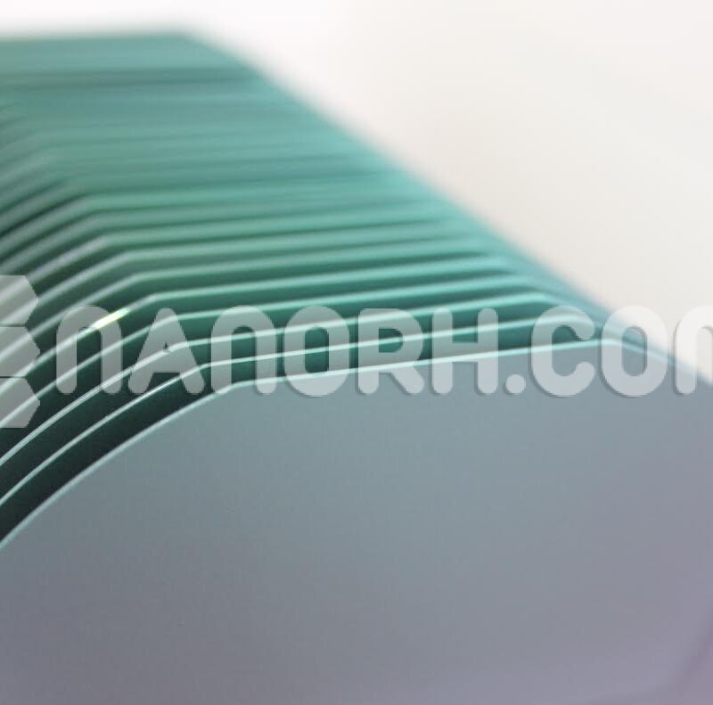
Triphenylamine Sputtering Target
Triphenylamine Sputtering Target
| Triphenylamine Sputtering Target | |
| Product No | NRE-43166 |
| CAS No. | 124729-98-2 |
| Formula | C57H48N4 |
| Molecular Weight | NA |
| Purity | >99 % |
| Density | NA |
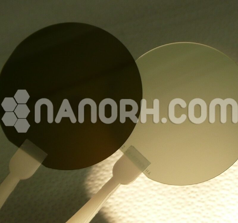
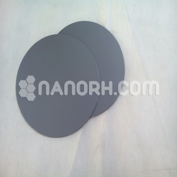
| Thickness | 3 mm (can be customized) |
| Diameter | 2 inch (can be customized) |
| Shape | Round |
| Resistivity | NA |
| Thermal Conductivity | NA |
Triphenylamine Sputtering Target
Introduction:
Triphenylamine sputtering target is an organic compound known for its unique electronic properties, making it an important material in organic electronics. TPA-based materials are used in various applications, particularly in organic light-emitting diodes (OLEDs), organic photovoltaics (OPVs), and as hole transport materials in organic semiconductors. Sputtering targets made from triphenylamine are used in physical vapor deposition (PVD) processes to create thin films with desirable electrical and optical characteristics.
Applications
Organic Light-Emitting Diodes (OLEDs): TPA is commonly used as a hole transport layer in OLEDs, improving charge injection and transport, which enhances device efficiency and brightness.
Organic Photovoltaics (OPVs): TPA-based materials are utilized in OPVs for their ability to facilitate charge transport, contributing to improved energy conversion efficiency.
Thin Film Transistors (TFTs): TPA can be used in the fabrication of organic thin film transistors, where its electronic properties help enhance performance.
Chemical Sensors: TPA-based films have potential applications in chemical sensing due to their sensitivity to various chemical environments.
Memory Devices: Research is exploring the use of TPA in organic memory devices, where its electronic properties can enable data storage applications.
Advantages
High Purity: Sputtering targets can be manufactured with high purity, ensuring high-quality films with consistent properties.
Tailored Electronic Properties: The composition and structure of TPA allow for the tuning of electronic properties to meet specific application needs.
Versatile Film Deposition: The PVD process enables the deposition of TPA films on a variety of substrates, making it suitable for different device architectures.