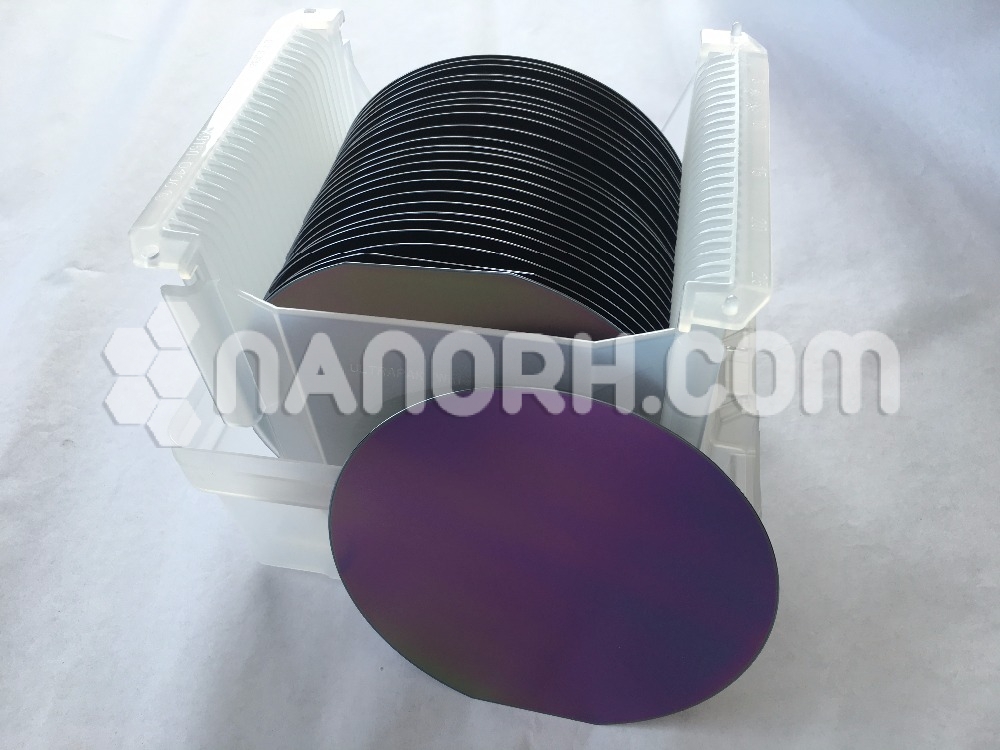
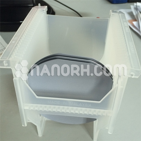
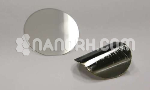
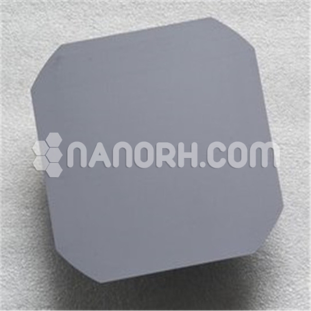
| Silicon Wafer Gold Coated | |
| Product No | NRE-44030 |
| CAS | NA |
| Type | NA |
| Crystal method | NA |
| Coating | Gold Coating |
| Diameter (mm) | 4” (101.6mm) |
| Thickness | 275 μm |
| RRG (%) | ≤12 % |
| Crystal Orientation | <100> |
| Oxygen Contents | 12.5-16.5 ppma |
| Carbon Contents | ≤1 ppma |
Silicon Wafer Gold Coated
Introduction:
Silicon wafer gold coated are specialized substrates used in various advanced applications. These wafers combine the excellent properties of silicon with a thin layer of gold, enhancing their functionality, particularly in electronic and optoelectronic devices. The gold coating provides superior electrical conductivity and corrosion resistance, making these wafers ideal for specific applications in semiconductor manufacturing and research.
Applications:
Semiconductor Devices:
Gold-coated wafers are used to create reliable electrical contacts in semiconductor components, improving the efficiency and performance of integrated circuits (ICs).
Microelectromechanical Systems (MEMS):
These wafers are vital in MEMS fabrication, serving as a platform for sensors and actuators where reliable electrical connections are crucial.
Optoelectronic Components:
In devices such as LEDs and photodetectors, the gold layer facilitates effective light coupling and enhances electrical performance, critical for efficient operation.
Biosensors:
Gold’s biocompatibility makes these wafers suitable for biomedical applications, including biosensors that require sensitive detection of biological interactions.
Surface Plasmon Resonance (SPR) Sensors:
Used in SPR technology for high-sensitivity biosensing applications, gold coatings enable the detection of low concentrations of biomolecules.
Research and Development:
In laboratory settings, 4-inch gold-coated silicon wafers are often utilized for experiments in nanotechnology, surface chemistry, and material science, providing a stable substrate for various applications.


