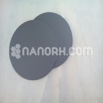
| Silicon Wafer 3 Inch | |
| Product No | NRE-44027 |
| CAS | 7440-21-3 |
| Type | P-Type |
| Crystal method | CZ |
| RRG (%) | ≤12 |
| Oxygen Contents (ppma) | 12.5-16.5 |
| Doping | Boron |
| Diameter (mm) | 3” (76.2mm) |
| Thickness | 250-500μm |
| Resistivity | 1-10ohm-cm |
| Surface | Both Side Polished |
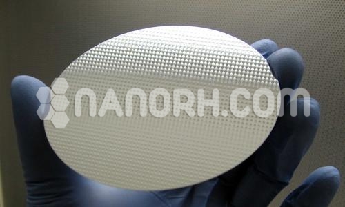
Silicon Wafer 3 Inch
Applications:
Silicon wafer 3 inch are commonly used in the semiconductor industry for various applications. Their size strikes a balance between manufacturing efficiency and cost-effectiveness, making them suitable for different technologies. Here are some key applications:
Integrated Circuits (ICs):
Silicon wafers 3 inch used in the fabrication of microprocessors, memory chips, and logic devices. 3-inch wafers are suitable for prototyping and small-scale production of ICs.
Sensors:
Employed in the production of various sensors, including temperature, pressure, and MEMS (Microelectromechanical Systems) sensors, leveraging silicon’s mechanical and electrical properties.
Photovoltaic Cells:
Used in the manufacture of solar cells, where silicon’s semiconductor properties are harnessed for converting solar energy into electrical energy.
Power Devices:
Suitable for manufacturing power semiconductor devices, including diodes and transistors, which are used in power management and conversion applications.
LEDs and Optoelectronic Devices:
Used as substrates for fabricating light-emitting diodes (LEDs) and other optoelectronic devices, where silicon’s properties can support efficient light generation.
Research and Development:
Commonly used in R&D laboratories for developing new semiconductor materials and devices, where smaller batch sizes are often required.
Surface Acoustic Wave (SAW) Devices:
Utilized in SAW devices for signal processing applications in telecommunications.
Microprocessors:
Suitable for low to mid-range performance microprocessors used in consumer electronics and embedded systems.


