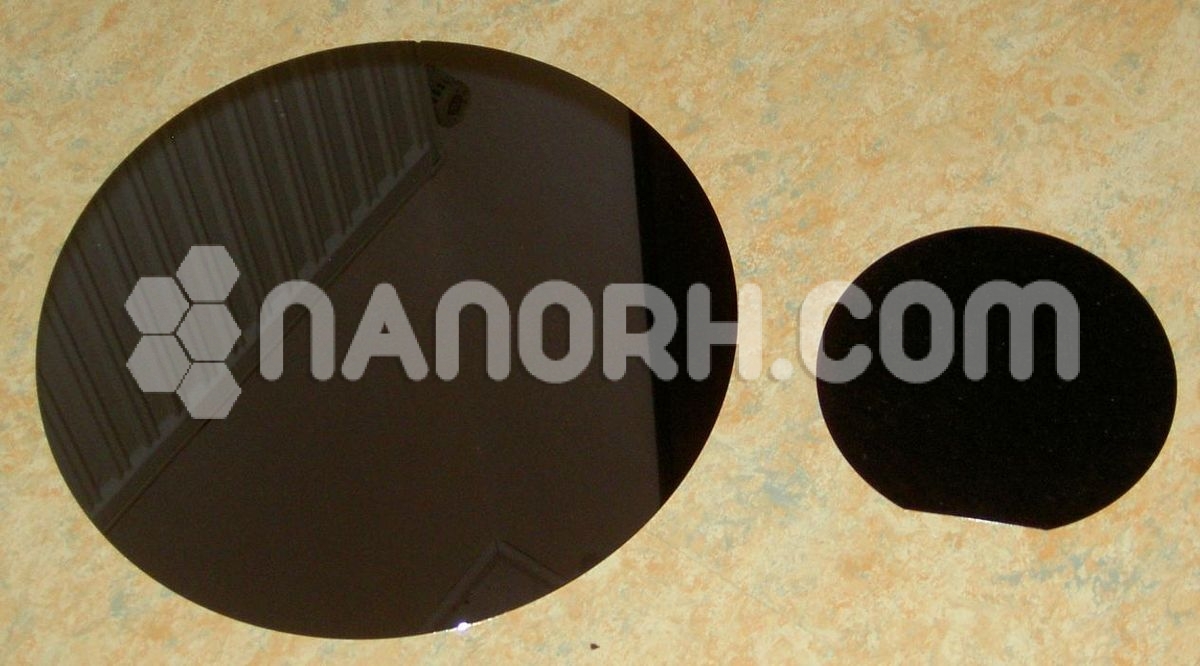
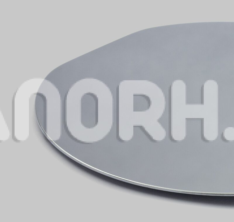
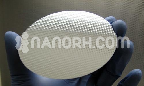
| P-Type Silicon Wafer 4 inch | |
| Product No | NRE-44018 |
| CAS | 7440-21-3 |
| Crystal method | CZ |
| Type | P-Type |
| Diameter (mm) | 4” (100.8mm) |
| Doping | Boron |
| Surface | Single Side Polished |
| Thickness | 250-500μm |
| Crystal Orientation | <100> |
| Resistivity | 1-10ohm-cm |
| RRG (%) | ≤12 |
| Oxygen Contents (ppma) | 12.5-16.5 |
P Type Silicon Wafer 4 inch
Introduction:
P type silicon wafer 4 inch are semiconductors that have been doped with elements such as boron, which create “holes” in the silicon lattice. These holes act as positive charge carriers, allowing for the conduction of electricity. A 4-inch diameter wafer is a common size used in the semiconductor industry, balancing efficiency and compatibility with various fabrication processes.
Properties:
Hole Conductivity: The introduction of boron creates holes in the silicon lattice, facilitating the movement of positive charge carriers.
Lower Electron Concentration: Compared to N-type silicon, P-type silicon has a lower concentration of electrons, making it suitable for forming p-n junctions.
Good Compatibility: P-type silicon wafers are compatible with standard semiconductor fabrication processes.
Applications
Integrated Circuits (ICs):
Used in the fabrication of various semiconductor devices, including microprocessors, memory chips, and analog components. P-type wafers are critical for creating complementary metal-oxide-semiconductor (CMOS) technology.
Solar Cells:
Employed in the production of photovoltaic devices, where P-type silicon forms the essential p-n junction for effective light absorption and charge separation.
Transistors:
Integral in the manufacturing of bipolar junction transistors (BJTs) and field-effect transistors (FETs), where P-type material serves as the emitter or base.
Diodes:
Used in the fabrication of various types of diodes, including rectifiers and light-emitting diodes (LEDs), leveraging the p-n junction properties.
Sensors:
Commonly found in temperature, pressure, and gas sensors, benefiting from their sensitivity and stability.
Microelectromechanical Systems (MEMS):
Employed in MEMS devices for applications in automotive, medical, and consumer electronics, where precise sensing and actuation are required.
Optoelectronic Devices:
Utilized in devices such as photodetectors and LEDs, where the unique properties of P-type silicon are essential for performance.


