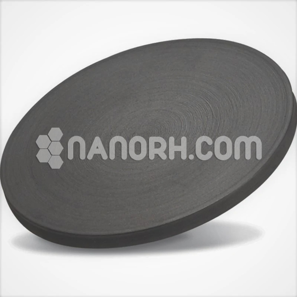
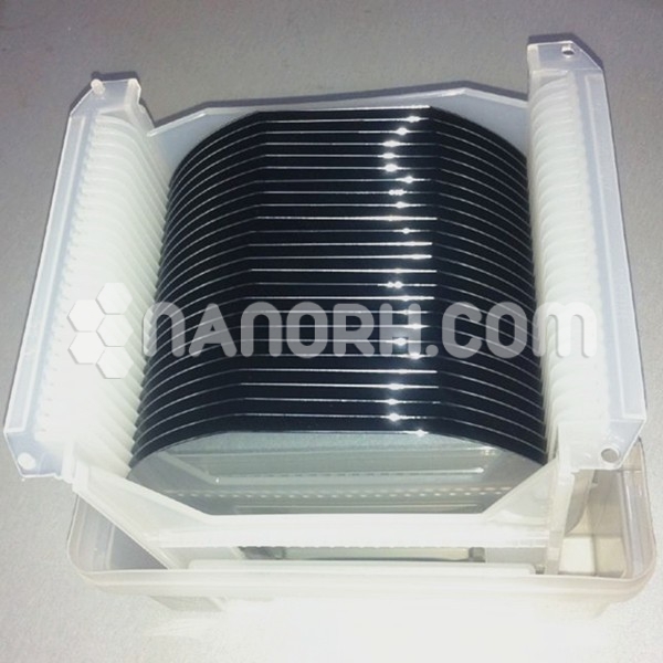
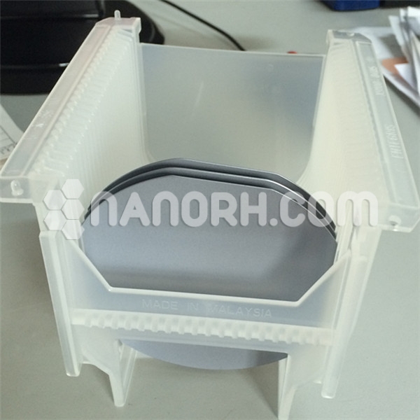
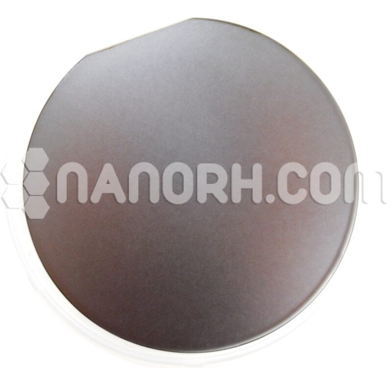
| Lead Selenide Sputtering Targets | |
| Product No | NRE-43480 |
| CAS No. | 12069-00-0 |
| Formula | PbSe |
| Molecular Weight | 286.16 |
| Purity | >99.9% |
| Density | NA |
| Thickness | 3 mm ± 0.5mm (can be customized) |
| Diameter | 50 mm ± 1mm (can be customized) |
| Shape | Round |
| Resistivity | NA |
| Thermal Conductivity | NA |
Lead Selenide Sputtering Targets
Introduction
Lead selenide (PbSe) is a semiconductor material known for its unique electronic and optical properties, particularly in the infrared spectrum. Sputtering targets made from lead selenide are utilized in physical vapor deposition (PVD) processes to create thin films for various applications.
Applications
Infrared Detectors: PbSe is widely used in infrared detectors due to its sensitivity to infrared radiation. This makes it suitable for applications in thermal imaging, gas sensing, and night vision technologies.
Photovoltaic Devices: Lead selenide is a promising material for thin-film solar cells, especially in the mid-infrared range, where it can improve energy conversion efficiency.
Optoelectronic Devices: PbSe is used in various optoelectronic applications, including lasers, light-emitting diodes (LEDs), and photodetectors, owing to its tunable bandgap.
Quantum Dots: Lead selenide quantum dots are explored for use in advanced display technologies and biological imaging, leveraging their size-tunable optical properties.
Thermoelectric Materials: Due to its favorable thermoelectric properties, PbSe can be used in thermoelectric devices for power generation and refrigeration applications.


