| Dummy Silicon Wafers 6″ | |
| Product No | NRE-44011 |
| Type | N-Type |
| Crystal method | CZ |
| Crystal Orientation | <100> |
| Thickness | 250-500μm |
| Diameter (mm) | 6” (152.4mm) |
| Doping | Phosphorous |
| Resistivity | 1-10ohm-cm |
| RRG (%) | ≤12 |
| Oxygen Contents (ppma) | 12.5-16.5 |
Dummy Silicon Wafers 6″
Introduction:
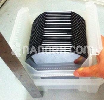
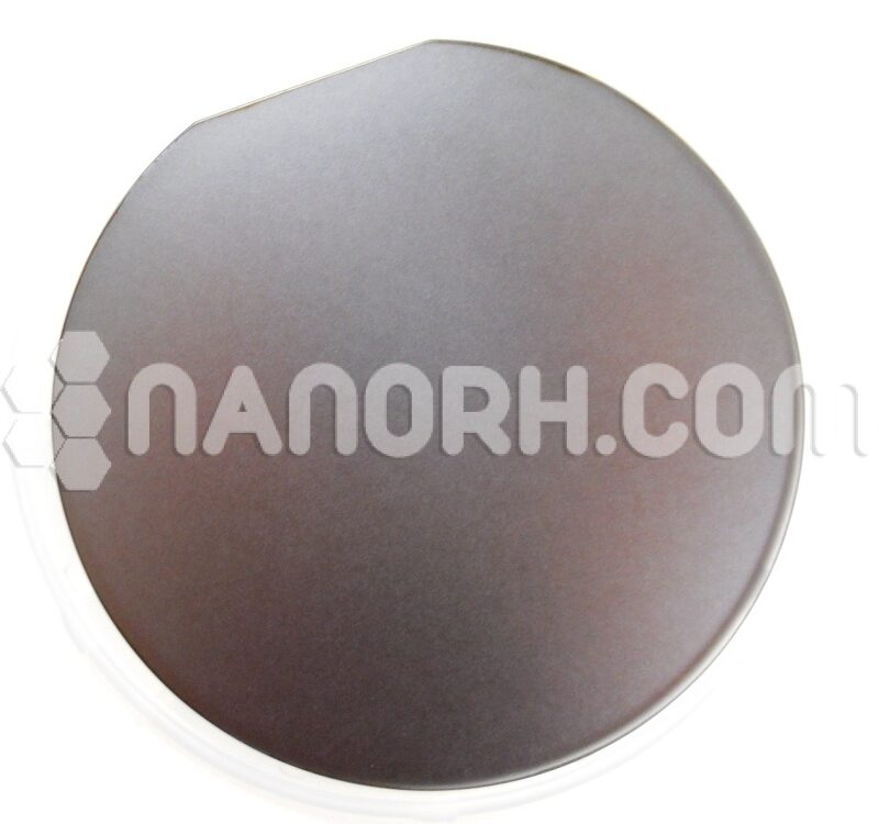
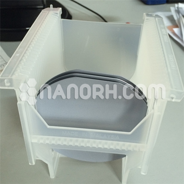
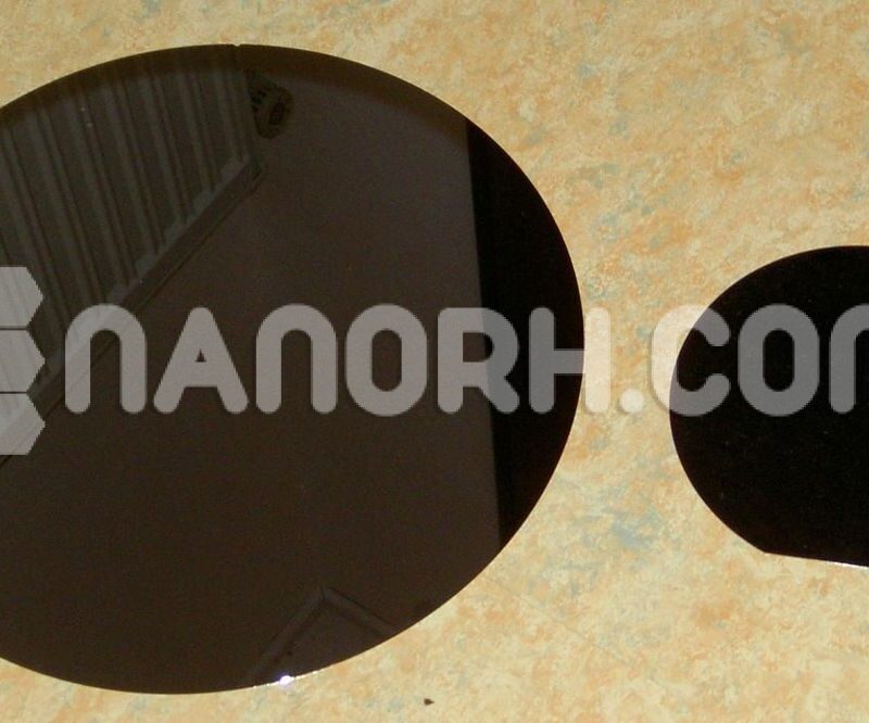
Dummy silicon wafers 6” also known as test wafers or carrier wafers, are silicon wafers that are typically used in semiconductor manufacturing for various non-active purposes. These wafers are often 6 inches in diameter and serve critical roles in processes such as fabrication, handling, and testing without being involved in actual device production. They are essential for maintaining the integrity of manufacturing processes and facilitating various experimental setups.
Properties
Material: Made from high-purity silicon, similar to active wafers, but not doped for specific electrical properties.
Surface Quality: Can be polished to a smooth finish, allowing for consistent handling and processing.
Size: The 6-inch diameter is commonly used in the industry, compatible with standard equipment and processes.
Applications
Process Development: Used in the development and optimization of fabrication processes, allowing engineers to test conditions without affecting production wafers.
Equipment Calibration: Serves as a reference for calibrating and tuning semiconductor manufacturing equipment, ensuring accurate results during production.
Material Handling: Facilitates the transport and handling of wafers through various manufacturing steps, protecting active wafers from contamination or damage.
Chemical Testing: Utilized in experiments involving etching, deposition, and other chemical processes to evaluate the effects of different chemicals on silicon.
Thermal Testing: Employed in thermal testing setups to measure temperature distribution and thermal performance in semiconductor processes.
Education and Training: Often used in academic and training environments for teaching semiconductor processing techniques without the risk of losing valuable active wafers.


