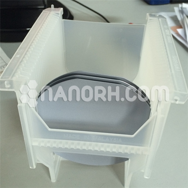
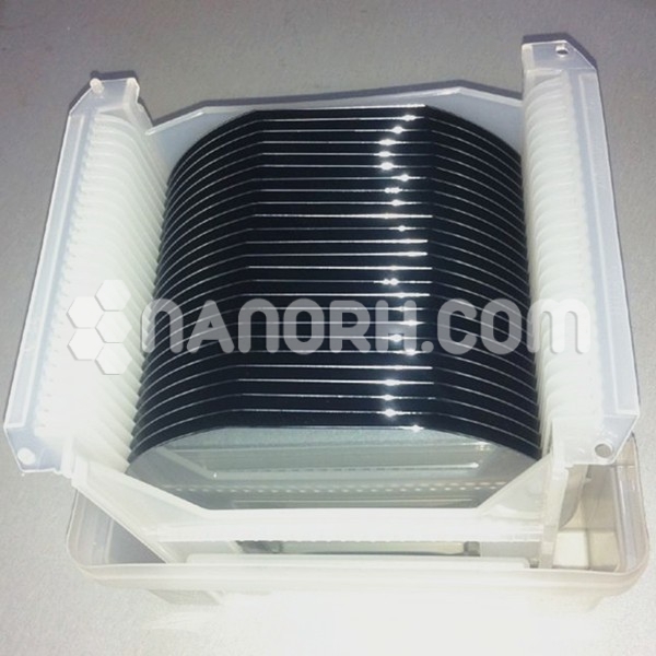
| CZ Silicon Wafer P-Type Boron Doped | |
| Product No | NRE-44007 |
| Type | P-Type |
| Formula | Zr |
| Crystal Orientation | <100> |
| Oxygen Contents | 12.5-16.5 |
| Thickness | 275 μm |
| Diameter (mm) | 10mm |
| Doping | Boron |
| Carbon Contents | ≤1 |
| RRG (%) | ≤12 |
| Surface | Single Side Polished |
CZ Silicon Wafer P-Type Boron Doped
CZ Silicon Wafer P-Type Boron Doped refers to silicon wafers produced using the Czochralski (CZ) method, which are doped with boron to create p-type silicon. These wafers have specific applications in the semiconductor industry and in technologies that rely on high-performance, stable, and efficient silicon materials. Here are the main applications of P-Type Boron Doped CZ Silicon Wafers:
Semiconductor Devices:
Transistors: P-type boron-doped silicon wafers are commonly used in the production of bipolar junction transistors (BJTs) and field-effect transistors (FETs). These devices rely on p-type silicon to form the base or the channel layer, essential for controlling the flow of current.
Diodes: P-type wafers are also used in the manufacturing of diodes, including rectifier diodes and Schottky diodes, which are critical in power conversion, signal processing, and electronic circuits.
Integrated Circuits (ICs): P-type silicon is used in CMOS (Complementary Metal-Oxide-Semiconductor) technology, where both n-type and p-type materials are required to create logic gates, memory devices, and other semiconductor components.
Solar Cells:
Photovoltaic (PV) Devices: P-type boron-doped silicon wafers are widely used in the manufacturing of solar cells. The boron doping creates the p-type layer of the silicon, which, when combined with the n-type layer, forms a p-n junction that is crucial for photovoltaic energy conversion. These wafers are used in both monocrystalline and multicrystalline solar panels.
High-Efficiency Solar Panels: P-type silicon wafers are typically used in high-efficiency solar cell technology because they offer better performance in terms of light absorption and charge separation, leading to higher energy conversion efficiencies.
Power Devices:
Power Transistors: P-type boron-doped silicon wafers are essential in the creation of power semiconductor devices, including power transistors and thyristors.


