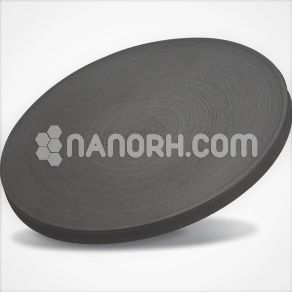
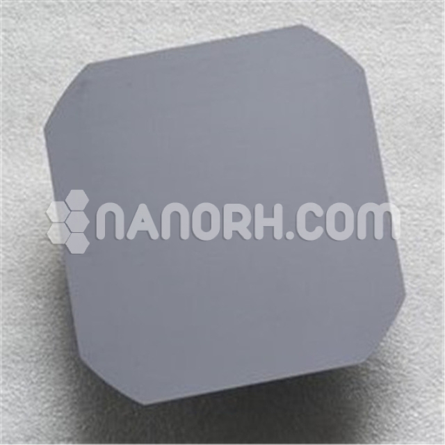
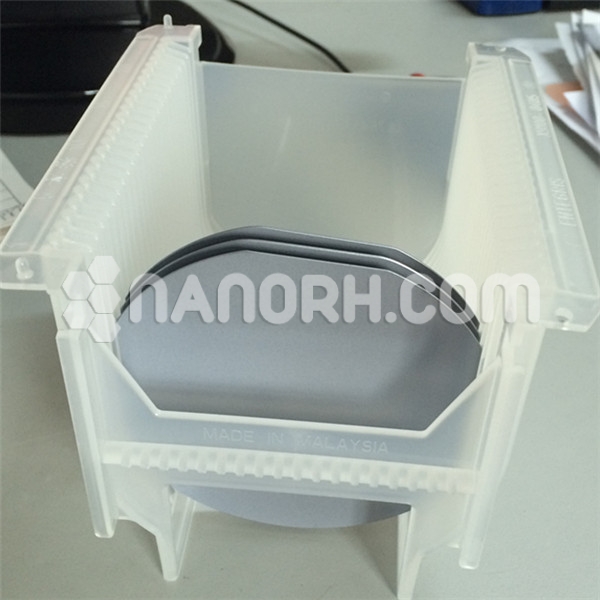
| Copper Indium Gallium Selenide Sputtering Targets | |
| Product No | NRE-43392 |
| CAS No. | NA |
| Formula | CIGS |
| Molecular Weight | NA |
| Purity | >99.9% |
| Density | 5.7 g/cm3 |
| Thickness | 3 mm ± 0.5mm (can be customized) |
| Diameter | 50 mm ± 1mm (can be customized) |
| Shape | Round |
| Resistivity | NA |
| Thermal Conductivity | NA |
Copper Indium Gallium Selenide Sputtering Targets
Copper Indium Gallium Selenide Sputtering Target Copper-indium (Cu-In) alloy sputtering targets are used in various advanced technological applications. Here’s a breakdown of their primary applications.
Semiconductor Fabrication
Interconnects and Contacts: Cu-In alloys are used in the semiconductor industry to create high-performance interconnects and contacts within integrated circuits. These alloys offer good electrical conductivity and thermal stability, which are crucial for efficient circuit operation.
Optoelectronic Devices
Thin-Film Solar Cells: Cu-In alloys are particularly significant in the production of thin-film solar cells, notably in the Cu(In,Ga)Se₂ (CIGS) solar cell technology. In this context, Cu-In alloys are used to deposit high-quality absorber layers, which are critical for the efficiency of the solar cells.
Light Emitting Devices: These alloys can also be used in optoelectronic devices, such as light-emitting diodes (LEDs) and laser diodes, where their specific properties can enhance device performance.
Thin-Film Transistors (TFTs)
Display Technology: In the production of thin-film transistors used in LCD and OLED displays, Cu-In alloys are used to create high-performance semiconductor layers. These layers are essential for the reliable operation of the displays.
Photovoltaic Cells
High-Efficiency Solar Panels: In addition to CIGS-based solar cells, Cu-In alloys are used in other types of photovoltaic technologies to enhance performance and efficiency. The alloy’s ability to form high-quality thin films is valuable for improving the performance of solar panels.
Research and Development
Material Science: Cu-In alloy sputtering targets are utilized in research to develop new materials and technologies. This includes exploring novel alloy compositions and sputtering techniques to optimize the properties of deposited films for various applications.
Coatings and Protective Layers
Protective Coatings: Cu-In alloys can be used to deposit coatings that provide protective layers or improve the durability of substrates. These coatings can enhance properties like corrosion resistance or wear resistance.
In these applications, the specific alloy composition and sputtering parameters are tailored to achieve the desired characteristics in the deposited films.


