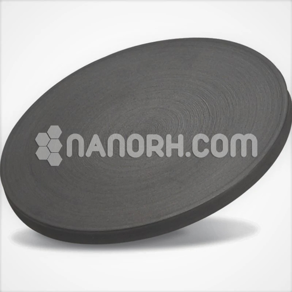
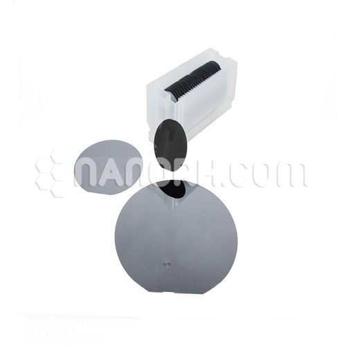
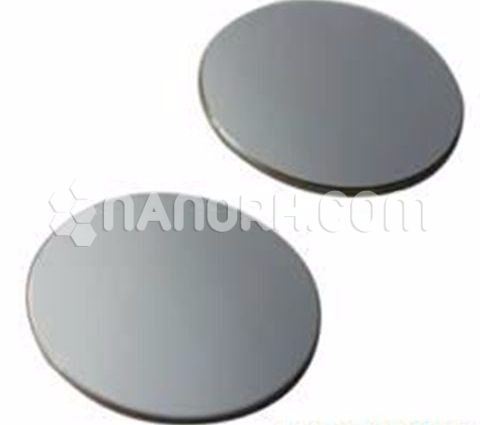
| Copper Gallium Selenide Sputtering Targets | |
| Product No | NRE-43390 |
| CAS No. | 12018-83-6 |
| Formula | CuGaSe2 |
| Molecular Weight | 291.19 |
| Purity | >99.9% |
| Density | 5.56 g/cm3 |
| Thickness | 3 mm ± 0.5mm (can be customized) |
| Diameter | 50 mm ± 1mm (can be customized) |
| Shape | Round |
| Resistivity | NA |
| Thermal Conductivity | NA |
Copper Gallium Selenide Sputtering Targets
Copper gallium selenide (CuGaSe₂) sputtering targets are primarily used in the production of high-efficiency thin-film solar cells. Here’s a detailed look at their key applications.
Photovoltaic Solar Cells:
Thin-Film Solar Panels: CuGaSe₂ is used to create high-efficiency thin-film solar cells. These solar cells are known for their ability to convert sunlight into electricity with high efficiency. The CuGaSe₂ material is an excellent absorber layer in thin-film solar cells, often used in conjunction with other materials to form a solar cell stack.
High-Efficiency Devices: CuGaSe₂-based solar cells can achieve high efficiencies, often exceeding those of some other thin-film technologies. This makes them attractive for use in high-performance solar panels.
Optoelectronic Devices:
Light Absorbers and Emitters: CuGaSe₂ can be used in various optoelectronic devices where efficient light absorption and emission are required. This includes applications in photodetectors and light-emitting devices.
Infrared Detectors:
Sensitive Infrared Devices: CuGaSe₂ can be employed in the fabrication of infrared detectors, which are used in a variety of applications, including thermal imaging and environmental monitoring.
High-Efficiency Photovoltaic Cells:
Multi-Junction Cells: In advanced photovoltaic applications, CuGaSe₂ may be used in multi-junction solar cells, where it serves as one of the layers in a stack of semiconductors to capture different parts of the solar spectrum.
Research and Development:
Material Science: CuGaSe₂ targets are used in research settings to explore and develop new materials and technologies for energy applications, including the optimization of photovoltaic devices and the development of new semiconductor materials.
The use of CuGaSe₂ sputtering targets involves depositing thin films of this material onto substrates to form the active layers of these devices.


