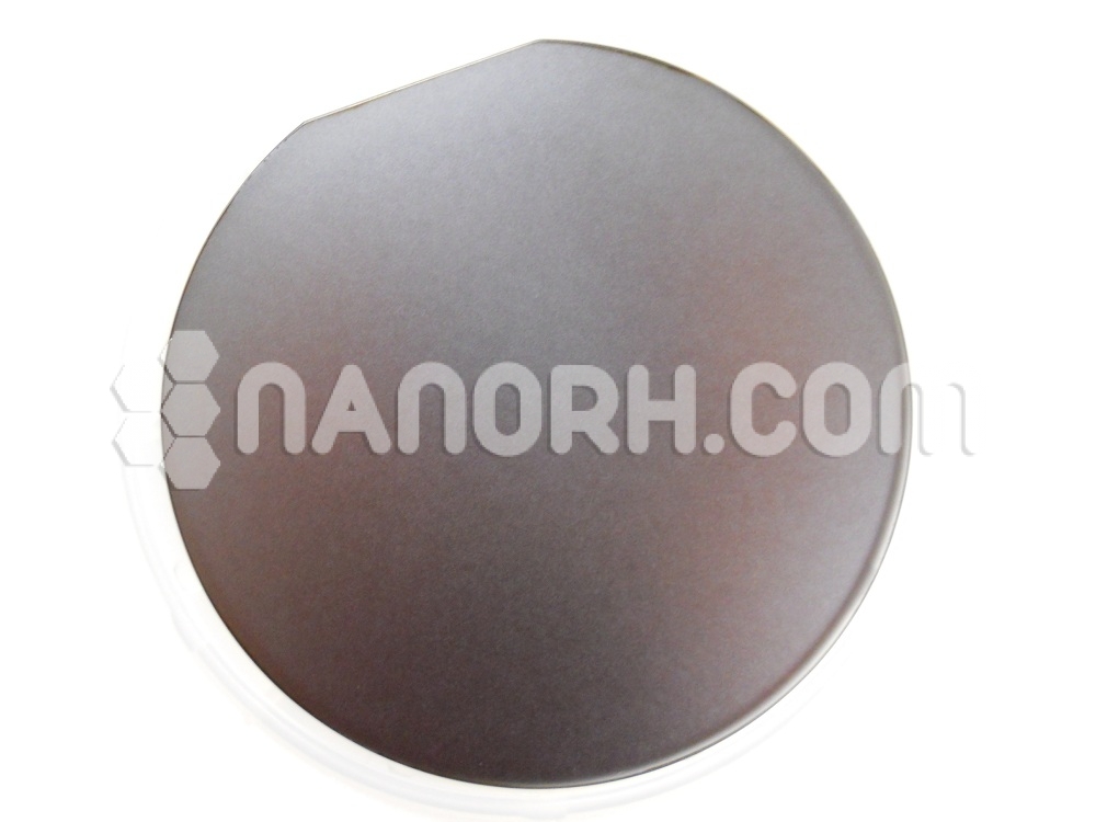
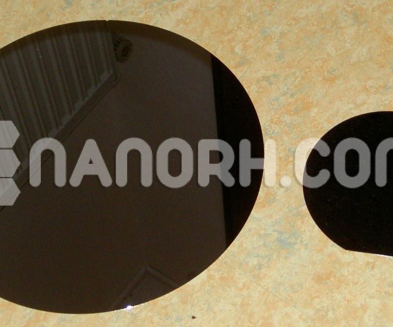
| 4 inch silicon wafer | |
| Product No | NRE-44002 |
| Type | N-Type |
| Formula | Si |
| Crystal method | CZ |
| Purity | NA |
| Thickness | 250-500μm |
| Diameter (mm) | 4” (100.8mm) |
| Doping | Phosphorous |
| Resistivity | 1-10ohm-cm |
| RRG (%) | ≤12 |
4 inch silicon wafer
Introduction:
4 inch silicon wafer are widely used in the semiconductor industry and represent a critical step in the evolution of wafer sizes. These wafers serve as substrates for various electronic components and are particularly valued for their balance of cost-effectiveness and scalability. The 4-inch size is a transition point between smaller wafers, used for prototyping and small-scale applications, and larger wafers, which are often used in high-volume manufacturing.
Properties
Material Composition: Typically made from high-purity silicon, either single-crystal (Czochralski or Float Zone methods) or polycrystalline.
Doping: Can be either N-type or P-type, depending on the desired electrical characteristics and application.
Thickness: Usually ranges from 525 to 725 micro meters, providing strength while allowing for various processing techniques.
Applications
Integrated Circuits (ICs): Widely used in the manufacturing of microprocessors, an alog chips, and digital logic circuits.
Power Electronics: Essential for the production of power devices such as MOSFETs and IGBTs, which are crucial in energy management and conversion applications.
MEMS Devices: Used in microelectromechanical systems for sensors and actuators in automotive, medical, and consumer electronics.
Solar Cells: Employed in photovoltaic technologies, particularly in research and small-scale solar cell production.
LEDs and Optoelectronics: Utilized in the fabrication of light-emitting diodes and other optoelectronic components.
Research and Development: Commonly found in laboratories for experimental devices and technology development.


