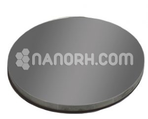
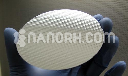
| Silicon Sputtering Target | |
| Product No | NRE-43141 |
| CAS No. | 7440-21-3 |
| Formula | Si |
| Molecular Weight | 28.085 g/mol |
| Purity | >99 % |
| Density | 2.32 g/cm³ |
| Thickness | 3 mm ± 0.5mm (can be customized) |
| Diameter | 50 mm ± 1mm (can be customized) |
| Shape | Round |
| Resistivity | NA |
| Thermal Conductivity | NA |
Silicon Sputtering Target
Introduction
Silicon sputtering targets are essential materials used in thin film deposition processes, particularly in the semiconductor, photovoltaic, and microelectronics industries. Silicon, as a fundamental element in electronic devices, is known for its excellent electrical properties, thermal conductivity, and abundance, making it a primary choice for various applications. Sputtering is a physical vapor deposition (PVD) technique that involves bombarding a target material with energetic particles, which then eject atoms that can be deposited onto a substrate to form a thin film.
Applications
Semiconductor Manufacturing: Silicon is crucial in the fabrication of semiconductor devices. Sputtered silicon films are used for various layers, including source/drain contacts, gate electrodes, and interconnects in integrated circuits. Its high purity and controlled deposition help ensure device performance and reliability.
Thin-Film Solar Cells: In photovoltaic applications, silicon sputtering targets are used to create layers in thin-film solar cells. These films contribute to the active layer of solar panels, enhancing light absorption and energy conversion efficiency.
Microelectromechanical Systems (MEMS): Silicon films deposited from sputtering targets are widely used in MEMS fabrication. They serve as structural layers in sensors, actuators, and other microdevices, benefiting from silicon’s mechanical properties.
Optical Coatings: Silicon can also be utilized in optical applications, such as creating thin films for optical filters and anti-reflective coatings. These coatings enhance the performance of lenses and optical devices by improving light transmission.
Thermal Barrier Coatings: In certain high-temperature applications, silicon films are applied as thermal barrier coatings to protect underlying materials from heat damage.


