| Cadmium Sputtering Targets | |
| Product No | NRE-43022 |
| CAS No. | 7440-43-9 |
| Formula | Cd |
| Molecular Weight | 112.41 g/mol |
| Purity | >99.9% |
| Density | 8.65 g/cm³ |
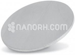
| Thickness | 3 mm ± 0.5mm (can be customized) |
| Diameter | 50 mm ± 1mm (can be customized) |
| Shape | Round |
| Resistivity | NA |
| Electronegativity | NA |
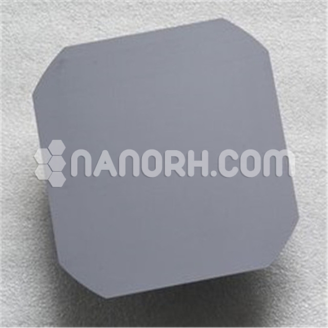
Cadmium Sputtering Targets
Cadmium sputtering targets are used in various applications within the field of thin film deposition and material science.
Applications
Semiconductors: Cadmium is often used in the production of semiconductors, especially in the creation of thin films for photovoltaic cells, such as Cadmium Telluride (CdTe) solar cells. CdTe is known for its efficiency in converting sunlight into electricity.
Optoelectronics: In optoelectronic devices, cadmium sputtering targets can be used to deposit thin films that are part of light-emitting devices or photodetectors.
Electronic Components: Cadmium films can be used in various electronic components due to their specific electrical properties.
Protective Coatings: In some cases, cadmium is used to create protective coatings on other metals to prevent corrosion, though its use has become less common due to environmental and health concerns.
Photovoltaic Cells (CdTe Solar Cells)
Application: Cadmium Telluride (CdTe) solar cells are a prominent use of cadmium sputtering targets. These cells are known for their efficiency in converting sunlight into electrical energy.
Process: Cd are used to deposit a layer of cadmium onto a substrate, which is then reacted with tellurium to form the CdTe layer.
Semiconductor Devices
Application: Cd compounds are used in the manufacturing of various semiconductor devices, including light sensors and thin-film transistors.
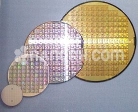
Process: Cadmium sputtering targets are used to create thin films of cadmium compounds on semiconductor wafers.
Optoelectronic Devices
Application: Cadmium compounds, such as Cadmium Sulfide (CdS), are used in optoelectronic devices like photodetectors and light-emitting diodes (LEDs).
Process: The sputtering targets are used to deposit thin layers of cadmium compounds that are essential for the functionality of these devices.
Thermoelectric Materials
Application: Cadmium-based materials are sometimes used in thermoelectric devices, which convert temperature differences into electrical voltage.
Process: Cd are used to deposit films that form part of the thermoelectric material.
Magnetic and Optical Thin Films
Application: Cadmium can be used in the creation of magnetic or optical thin films for specialized applications.
Process: Cd are employed to deposit thin films with specific magnetic or optical properties.


