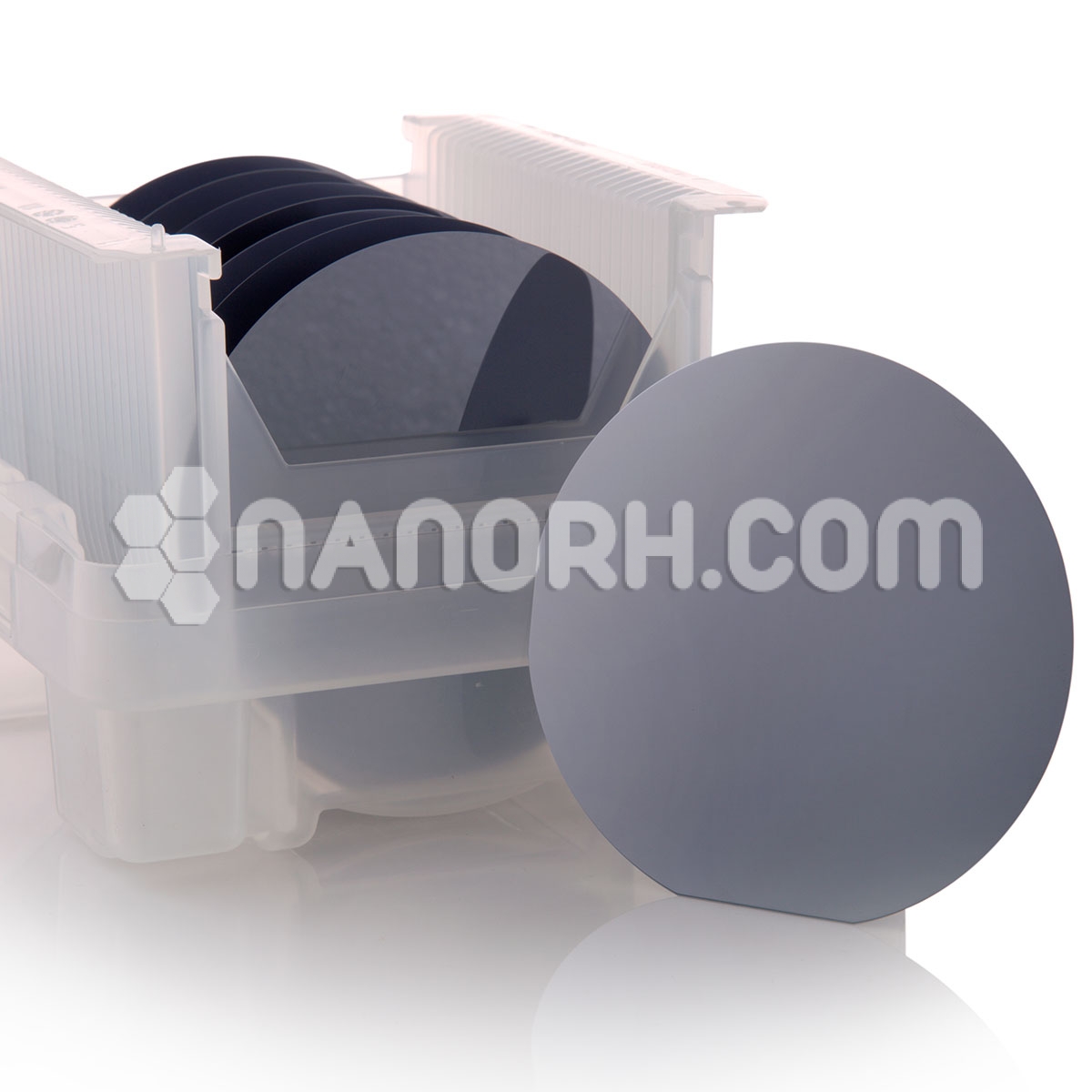
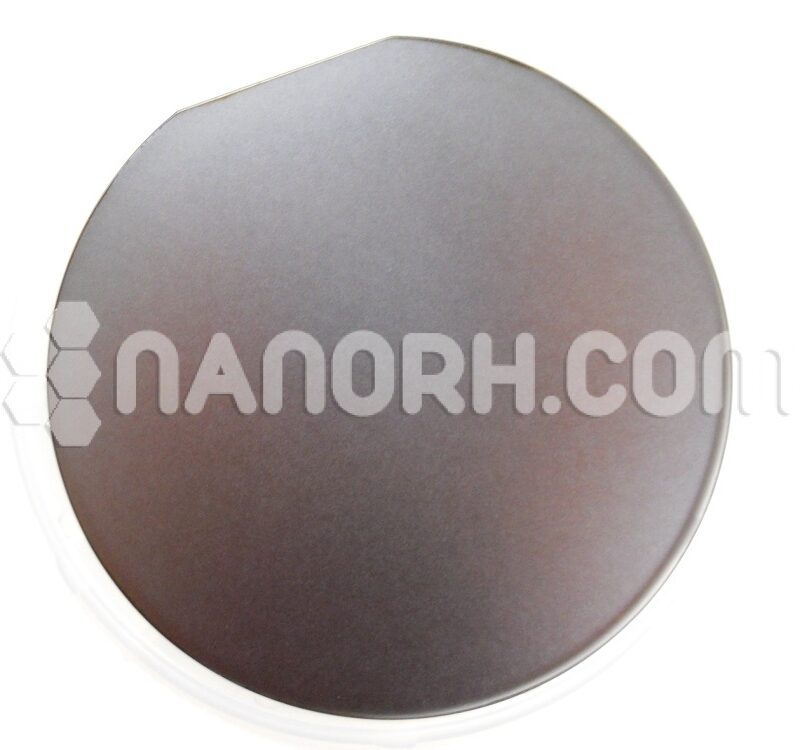
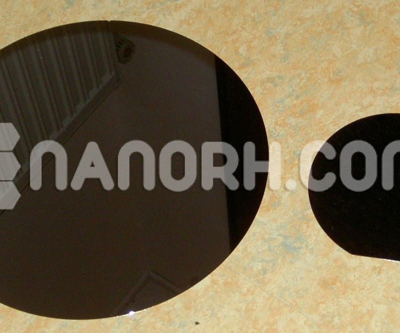
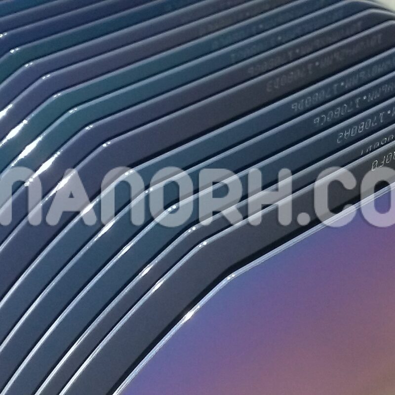
| P-Type Silicon Wafers | |
| Product No | NRE-44019 |
| CAS | 7440-21-3 |
| Crystal method | CZ |
| Type | P-Type |
| Diameter (mm) | 4” (100mm) |
| Doping | Boron |
| Surface | Single Side Polished |
| Thickness | 250-500μm |
| Crystal Orientation | <100> |
| Resistivity | 1-10ohm-cm |
| RRG (%) | ≤12 |
| Oxygen Contents (ppma) | 12.5-16.5 |
P Type Silicon Wafers
Introduction:
P type silicon wafers, particularly those doping with boron, are essential components in semiconductor technology. Boron doping introduces holes into the silicon lattice, which serve as positive charge carriers, enabling electrical conduction. The 4-inch diameter of these wafers is a standard size in the industry, facilitating efficient processing and integration into various electronic devices.
Properties:
Hole Conduction: The doping with boron creates an abundance of holes, enhancing the material’s ability to conduct electricity.
Shallow Acceptors: Boron acts as a shallow acceptor, allowing for easier excitation of holes into the conduction band, improving conductivity.
Compatibility: These wafers are compatible with standard semiconductor fabrication techniques, making them versatile for various applications.
Applications of Boron-Doping P-Type Silicon Wafers
Integrated Circuits (ICs):
Used in the fabrication of microprocessors, memory devices, and analog circuits, where the p-n junctions formed with N-type silicon are crucial for device operation.
Solar Cells:
Integral in the production of photovoltaic devices, where boron-doping P-type silicon is essential for forming efficient p-n junctions that facilitate light absorption and electron-hole separation.
Bipolar Junction Transistors (BJTs):
Employed in BJTs, where P-type silicon serves as the base or emitter, enhancing amplification and switching capabilities.
Diodes:
Utilized in various diode applications, including rectifiers and light-emitting diodes (LEDs), benefiting from the properties of the p-n junction.
Sensors:
Commonly found in temperature, pressure, and gas sensors, leveraging the sensitivity of P-type silicon to external environmental changes.
Microelectromechanical Systems (MEMS):
Used in MEMS devices for applications in automotive, medical, and consumer electronics, where precise sensing and actuation are necessary.
Optoelectronic Devices:
Employed in devices such as photodetectors and LEDs, where P-type silicon plays a crucial role in device performance and efficiency.


