| Heavily Doped Silicon Wafer | |
| Product No | NRE-44013 |
| Type | N-Type |
| Crystal method | CZ |
| Crystal Orientation | 12.5-16.5 ppma |
| Thickness | 275 μm |
| Diameter (mm) | 2” (50.8mm) |
| Doping | Boron |
| Resistivity | 1-10ohm-cm |
| Surface | Both Side Polished |
| RRG (%) | ≤12 % |
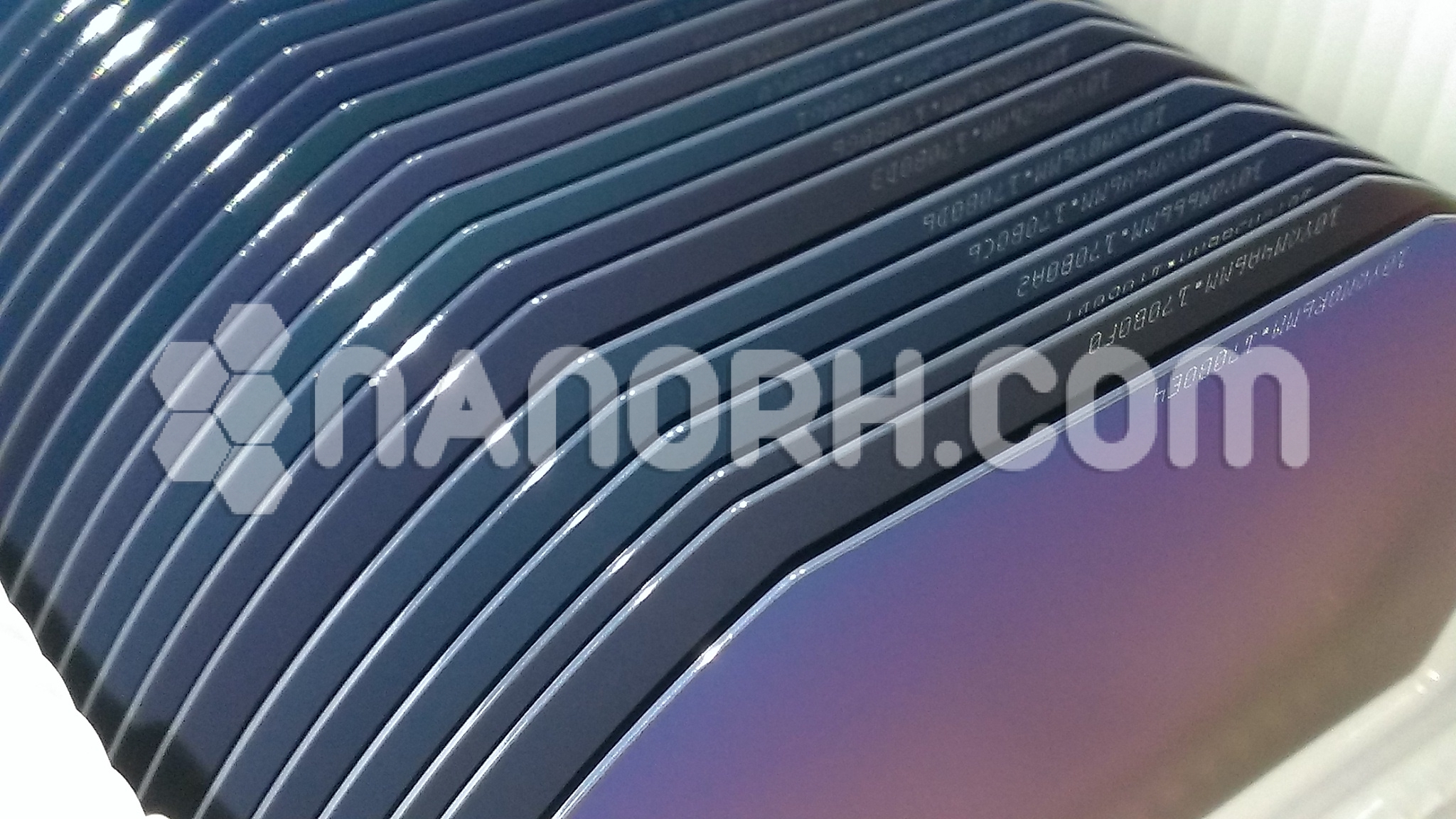
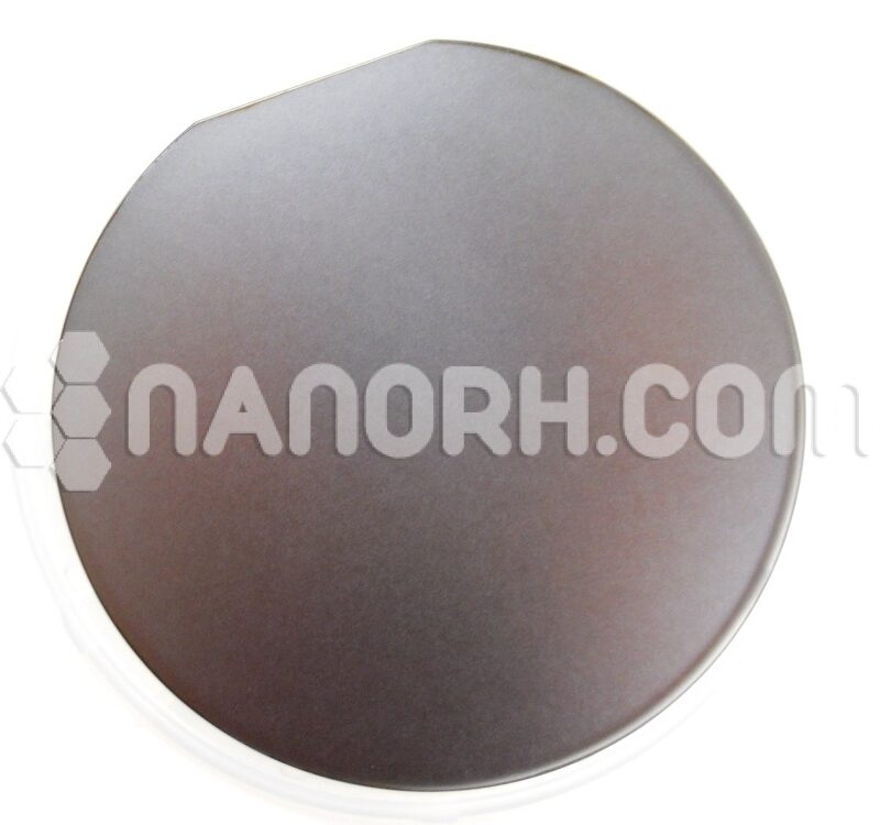
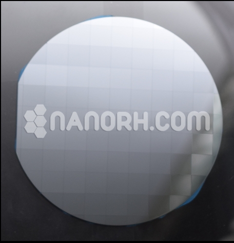
Heavily Doped Silicon Wafer
Introduction:
Heavily doped silicon wafer are silicon substrates intentionally infused with a high concentration of donor impurities, typically phosphorus. These wafers, commonly with a diameter of 2 inches, exhibit enhanced electrical conductivity due to an abundance of free electrons, making them crucial for various semiconductor applications. The increased doping concentration alters the material’s electrical properties, enabling specific functions in electronic devices.
Properties
High Electron Concentration: The heavy doping introduces a significant number of free electrons, resulting in enhanced electrical conductivity.
Reduced Resistivity: The resistivity of heavily doped N-type wafers is significantly lower than that of lightly doped silicon, facilitating better performance in applications that require efficient charge transport.
Substrate Quality: While the doping concentration enhances conductivity, it can also impact the crystal structure, so maintaining a balance between doping levels and crystal quality is essential.
Applications
Integrated Circuits (ICs): Used in the fabrication of high-performance transistors and logic devices, where low resistivity is critical for speed and efficiency.
Power Devices: Employed in the manufacturing of power transistors and diodes, facilitating efficient energy management and switching applications.
Contact and Interconnects: Used as low-resistance contacts or interconnects in semiconductor devices, improving overall electrical performance.
Sensors: Suitable for applications in gas and temperature sensors, leveraging their electrical properties to enhance sensitivity.
Bipolar Junction Transistors (BJTs): Integral in the fabrication of BJTs, where heavily doped N-type regions are essential for device operation.
Research and Development: Frequently used in experimental setups and research for testing new semiconductor materials and devices.


