| Phosphorus Doped Silicon Wafer | |
| Product No | NRE-44021 |
| CAS | NA |
| Crystal method | CZ |
| Type | N-Type |
| Diameter (mm) | 4″ (101.6mm) |
| Doping | Phosphorous |
| Thickness | 250-500μm |
| Crystal Orientation | <100> |
| Resistivity | 1-10ohm-cm |
| RRG (%) | ≤12 % |
| Oxygen Contents (ppma) | 12.5-16.5 |
Phosphorus Doped Silicon Wafer
Introduction:
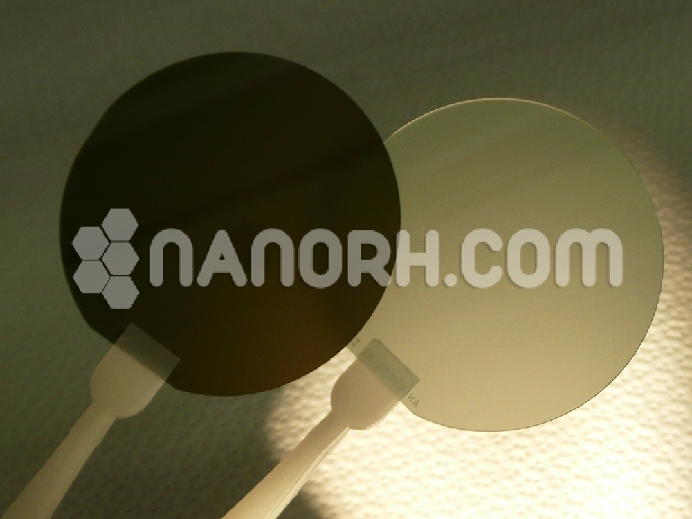
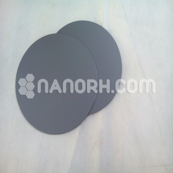
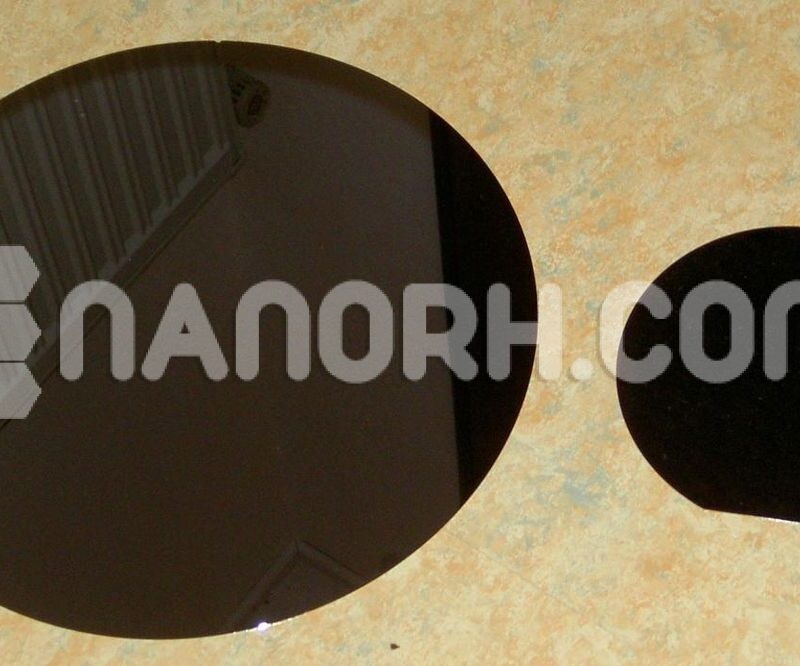
Phosphorus doped silicon wafer are a type of N-type semiconductor material created by introducing phosphorus atoms into the silicon lattice. This doping process increases the number of free electrons available for conduction, enhancing the material’s electrical properties. The 4-inch diameter wafers are commonly used in the semiconductor industry, offering a balance between efficient production and integration into various electronic devices.
Properties
High Electron Concentration: Phosphorus acts as a donor, providing extra electrons that significantly increase the electrical conductivity of the silicon.
Shallow Donor Levels: The doping creates energy levels close to the conduction band, allowing for easier excitation of electrons, facilitating efficient charge transport.
Good Thermal Stability: These wafers exhibit excellent thermal stability, making them suitable for various electronic applications.
Applications)
Integrated Circuits (ICs):
Used extensively in the production of microprocessors, memory chips, and logic devices. The high conductivity of phosphorus-doped silicon enhances the performance and speed of these components.
Power Electronics:
Employed in the manufacturing of power transistors, diodes, and rectifiers, where efficient electron flow is essential for energy conversion and management.
Photovoltaic Cells:
Integral in the fabrication of solar cells, particularly for forming p-n junctions that are crucial for effective light absorption and conversion of solar energy into electricity.
Bipolar Junction Transistors (BJTs):
Utilized in the production of BJTs, where the N-type silicon serves as the collector or emitter, enhancing performance in amplification and switching applications.
Microelectromechanical Systems (MEMS):
Used in MEMS devices for applications such as sensors and actuators, taking advantage of the material’s electrical properties for precise operation.
Gas and Temperature Sensors:
Employed in various sensor applications that require sensitivity to environmental changes, leveraging the responsiveness of N-type silicon.
Radio-Frequency Identification (RFID):
Used in RFID technology, benefiting from the reliable conductivity and performance of phosphorus-doped silicon in communication applications.


