| Silicon Wafer Gold Coated | |
| Product No | NRE-44030 |
| CAS | NA |
| Type | NA |
| Crystal method | NA |
| Coating | Gold Coating |
| Diameter (mm) | 4” (101.6mm) |
| Thickness | 275 μm |
| RRG (%) | ≤12 % |
| Crystal Orientation | <100> |
| Oxygen Contents | 12.5-16.5 ppma |
| Carbon Contents | ≤1 ppma |
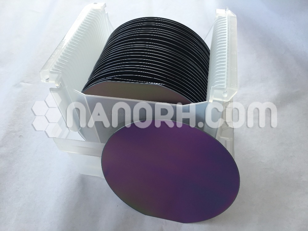
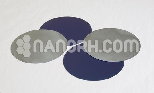
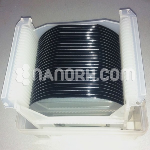
Silicon Wafer Gold Coated
Introduction:
Silicon wafer gold coated substrates that have been coated with a thin layer of gold. This specialized treatment enhances the properties of the silicon wafer, making it suitable for a range of advanced applications. Gold is chosen for its excellent electrical conductivity, corrosion resistance, and ability to form stable and reliable contacts with silicon.
Applications:
Semiconductor Devices:
Gold coatings provide effective electrical contacts in various semiconductor devices, ensuring reliable connections and improved performance in integrated circuits (ICs).
Microelectromechanical Systems (MEMS):
In MEMS fabrication, gold coatings can be used for electrical interconnects, enhancing device reliability and performance. They are particularly useful in sensors and actuators.
Optoelectronics:
Gold-coated wafers are used in optoelectronic applications, such as light-emitting diodes (LEDs) and photodetectors, where efficient light coupling and electrical connectivity are essential.
Biomedical Applications:
The biocompatibility of gold makes these wafers suitable for use in biosensors and other biomedical devices. They can facilitate improved signal transduction and biological interactions.
Surface Plasmon Resonance (SPR) Sensors:
Gold coatings enable SPR techniques for biosensing applications. These sensors leverage the unique optical properties of gold to detect biological interactions at very low concentrations.
Research and Development:
In laboratory settings, gold-coated silicon wafers are often used in research involving surface chemistry, nanotechnology, and material science, providing a stable platform for experimentation.


