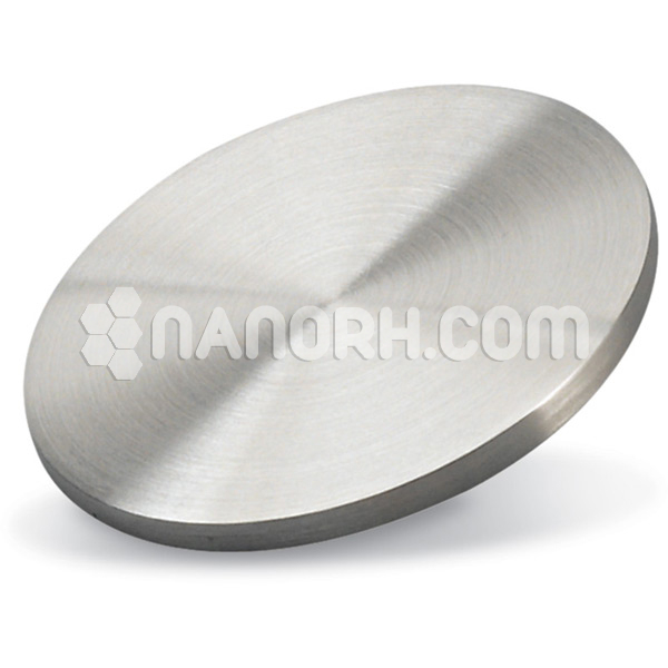
| Tin Arsenide Sputtering Targets | |
| Product No | NRE-43572 |
| CAS No. | 39332-13-3 |
| Formula | SnAs |
| Molecular Weight | 193.61 |
| Purity | >99.9% |
| Density | NA |
| Thickness | 3 mm ± 0.5mm (can be customized) |
| Diameter | 50 mm ± 1mm (can be customized) |
| Shape | Round |
| Resistivity | NA |
| Thermal Conductivity | NA |
Tin Arsenide Sputtering Targets
Tin arsenide sputtering targets is a compound with notable semiconductor properties, making it suitable for various advanced applications. Here are some key applications of tin arsenide sputtering targets.
Semiconductor Devices:
SnAs can be used in the fabrication of semiconductor devices, including transistors and diodes, due to its suitable bandgap and electronic properties.
Infrared Detectors:
Tin arsenide is effective in infrared detection applications. Its ability to absorb and respond to infrared radiation makes it valuable for thermal imaging, spectroscopy, and sensing technologies.
Optoelectronic Devices:
SnAs can be employed in optoelectronic applications, including light-emitting diodes (LEDs) and laser diodes, particularly in the mid-infrared range.
Thermoelectric Applications:
Due to its thermoelectric properties, SnAs can be utilized in thermoelectric devices for efficient energy conversion, particularly in low to moderate temperature ranges.
Thin-Film Transistors:
Tin arsenide is also investigated for use in thin-film transistors (TFTs), which are essential components in displays and flexible electronics.
Research and Development:
SnAs is of interest in research related to quantum materials and advanced electronic structures, providing insights into new materials for future technologies.
Sputtering Process
The sputtering process for tin arsenide involves using a SnAs target, which, when bombarded with ions, releases atoms for deposition onto substrates.


