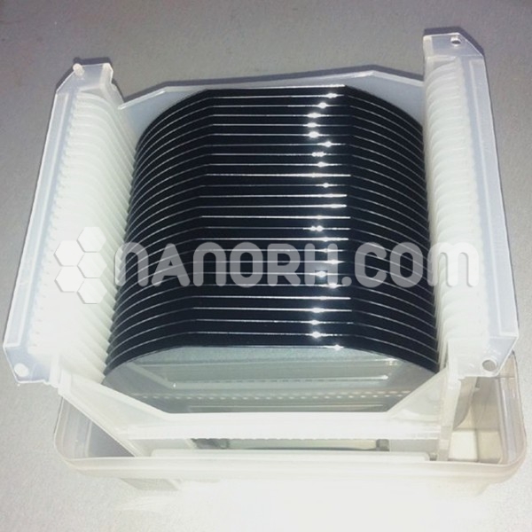
Thulium Telluride Sputtering Targets
Thulium Telluride Sputtering Targets
| Thulium Telluride Sputtering Targets | |
| Product No | NRE-43570 |
| CAS No. | 12040-14-1 |
| Formula | TmTe |
| Molecular Weight | 296.53 |
| Purity | >99.9% |
| Density | 9.36 g/cm3 |
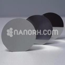
| Thickness | 3 mm ± 0.5mm (can be customized) |
| Diameter | 50 mm ± 1mm (can be customized) |
| Shape | Round |
| Resistivity | NA |
| Thermal Conductivity | NA |
Thulium Telluride Sputtering Targets
Thulium telluride Sputtering Targets is a compound of thulium and tellurium that has garnered interest for its unique properties, making it suitable for various advanced applications, particularly in thin film technology. Here are some key applications of thulium telluride sputtering targets.
Thermoelectric Materials:
TmTe exhibits promising thermoelectric properties, allowing for efficient conversion between heat and electricity. It can be used in thermoelectric generators and coolers, making it valuable in energy harvesting and temperature management applications.
Optoelectronics:
Thulium telluride is explored for its optoelectronic properties, particularly in mid-infrared photodetectors and light-emitting devices. Its ability to form high-quality thin films is essential for developing efficient optoelectronic components.
Topological Insulators:
TmTe is studied for its potential as a topological insulator, which can enable advanced electronic applications and quantum computing. Thin films of TmTe could be used to explore quantum states and electron transport properties.
Infrared Sensors:
Due to its semiconductor properties and ability to operate in the infrared range, TmTe can be used in the fabrication of infrared sensors and detectors, which are essential in various imaging and sensing technologies.
Spintronic Devices:
The magnetic and electronic properties of thulium telluride make it a candidate for spintronic applications, where the electron’s spin is exploited for information processing and storage.
Sputtering Process
The sputtering process for thulium telluride involves using a target of the compound, which, when bombarded with ions, releases atoms that can then be deposited onto substrates. This method allows for precise control over film thickness and composition, which is crucial for optimizing the performance of the resulting materials.