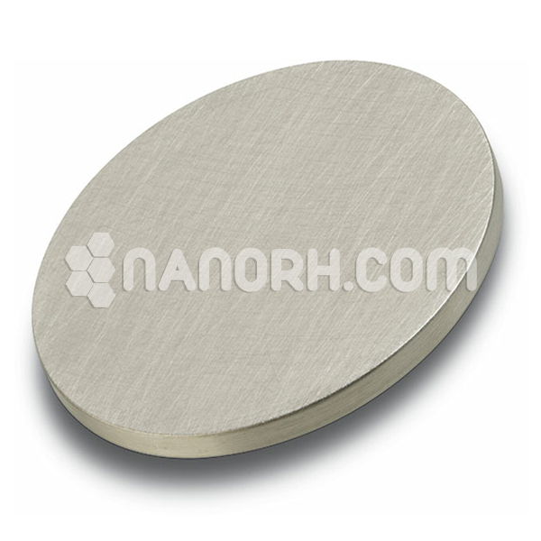
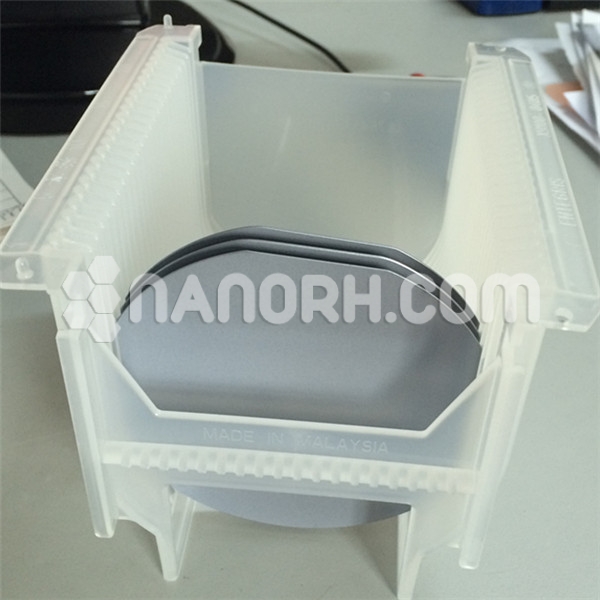
| Cadmium Fluoride Sputtering Targets | |
| Product No | NRE-43345 |
| CAS No. | 7790-79-6 |
| Formula | CdF2 |
| Molecular Weight | 150.41 |
| Purity | >99.9% |
| Density | 6.33 g/cm3 |
| Thickness | 3 mm ± 0.5mm (can be customized) |
| Diameter | 50 mm ± 1mm (can be customized) |
| Shape | Round |
| Resistivity | NA |
| Thermal Conductivity | NA |
Cadmium Fluoride Sputtering Targets
Cadmium fluoride (CdF₂) sputtering targets are used to deposit thin films of cadmium fluoride, which can be applied in several advanced technologies due to its unique properties.
Optical Coatings
Anti-Reflective Coatings: Cadmium fluoride films are used to create anti-reflective coatings for optical lenses and other components. CdF₂ has a low refractive index, which makes it effective in reducing reflections and improving light transmission.
Optical Windows: CdF₂ coatings can be applied to optical windows to enhance their performance in various optical systems, including those used in high-precision imaging and laser applications.
High-Energy Laser Systems
Laser Components: CdF₂ is used in the fabrication of optical elements for high-energy laser systems. The material’s transparency to a wide range of wavelengths, including UV and infrared, makes it suitable for laser windows and lenses.
Laser Mirrors: Thin films of CdF₂ are used as coatings for laser mirrors due to their high damage threshold and stability under high-energy laser conditions.
Phosphor Materials
Phosphor Coatings: CdF₂ can be used in the production of phosphor materials, which are essential for applications such as display screens, fluorescent lighting, and X-ray imaging.
Semiconductor Devices
Insulating Layers: In semiconductor manufacturing, CdF₂ can be used as an insulating layer. Its electrical insulating properties make it suitable for applications where high dielectric strength is required.
Optoelectronic Devices
UV-Transparent Films: Cadmium fluoride’s transparency in the ultraviolet (UV) range makes it useful for UV-optical devices, such as UV sensors and detectors.
Thin-Film Transistors (TFTs)
Display Technology: CdF₂ sputtered films can be used in thin-film transistors for display technologies. Its insulating properties contribute to the performance of TFTs in LCDs and other display systems.
Research and Development
Material Science: CdF₂ sputtering targets are used in research to explore the properties and potential applications of cadmium fluoride. This includes investigating its use in new optical, electronic, and semiconductor technologies.


