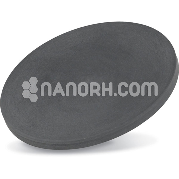
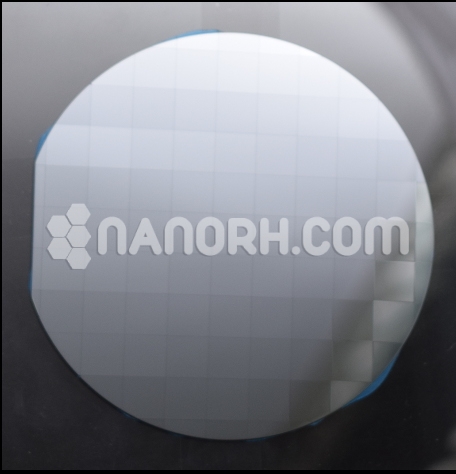
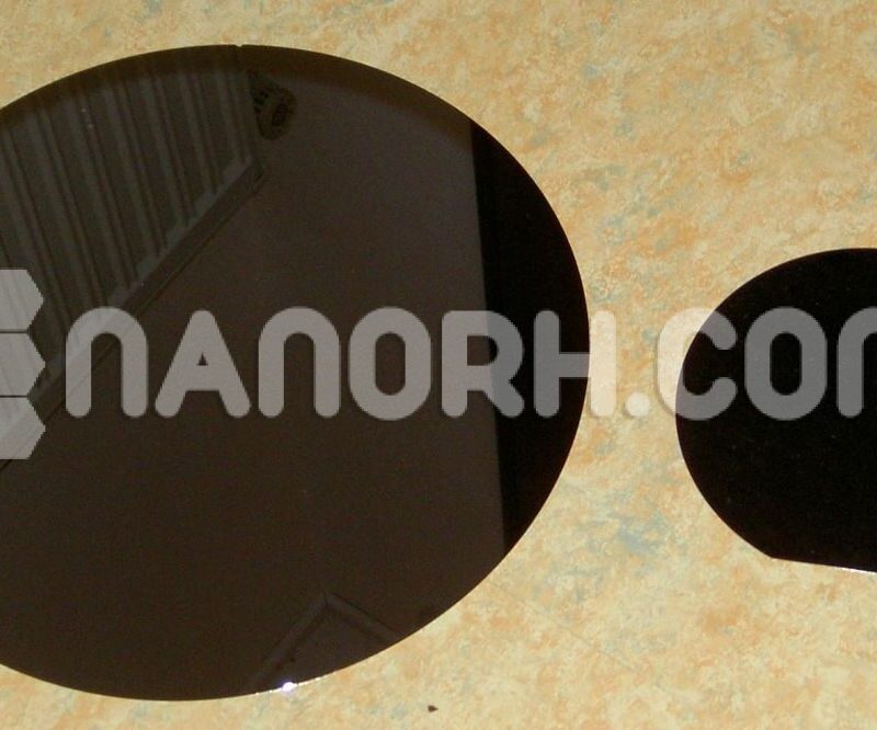
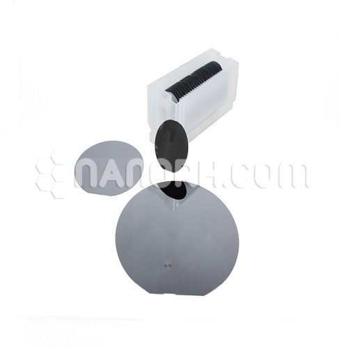
| Selenium Sputtering Targets | |
| Product No | NRE-43271 |
| CAS No. | 7782-49-2 |
| Formula | Se |
| Molecular Weight | 78.96 |
| Purity | >99.9% |
| Density | 4.79 g/cm3 |
| Thickness | 3 mm ± 0.5mm (can be customized) |
| Diameter | 50 mm ± 1mm (can be customized) |
| Shape | Round |
| Resistivity | NA |
| Thermal Conductivity | NA |
Selenium Sputtering Targets
Introduction:
Selenium sputtering targets are compounds formed with selenium (Se) and various metals, such as cadmium (Cd), indium (In), or gallium (Ga). selenium are often used in semiconductor applications and thin film technologies due to their unique electrical and optical properties.
Applications
Photovoltaic Devices:
Selenium particularly cadmium Selenium are widely used in thin-film solar cells. Their properties make them efficient for light absorption and conversion to electrical energy.
Optoelectronics:
Selenium compounds are employed in the production of light-emitting diodes (LEDs), laser diodes, and other optoelectronic devices, benefiting from their semiconductor properties.
Quantum Dots:
Used in the fabrication of quantum dots for applications in displays, lighting, and biological imaging. Cadmium selenium quantum dots, in particular, have exceptional photoluminescent properties.
Sensors:
Selenium can be utilized in gas sensors and photodetectors, where their sensitivity to light and specific gas interactions is beneficial.
Thin Film Transistors (TFTs):
Employed in the manufacture of TFTs for display technologies, such as LCDs and OLEDs, leveraging their electrical conductivity and stability.
Research and Development:
Selenium sputtering targets are used in various research settings to explore new materials and optimie processes in semiconductor physics and material science.
Thermoelectric Devices:
Investigated for use in thermoelectric materials, where their ability to convert temperature differences into electric voltage is valuable for energy harvesting.


